- 您现在的位置:买卖IC网 > Sheet目录329 > IDT71016S20YGI (IDT, Integrated Device Technology Inc)IC SRAM 1MBIT 20NS 44SOJ
IDT71016, CMOS Static RAM
1 Meg (64K x 16-bit)
Commercial and Industrial Temperature Ranges
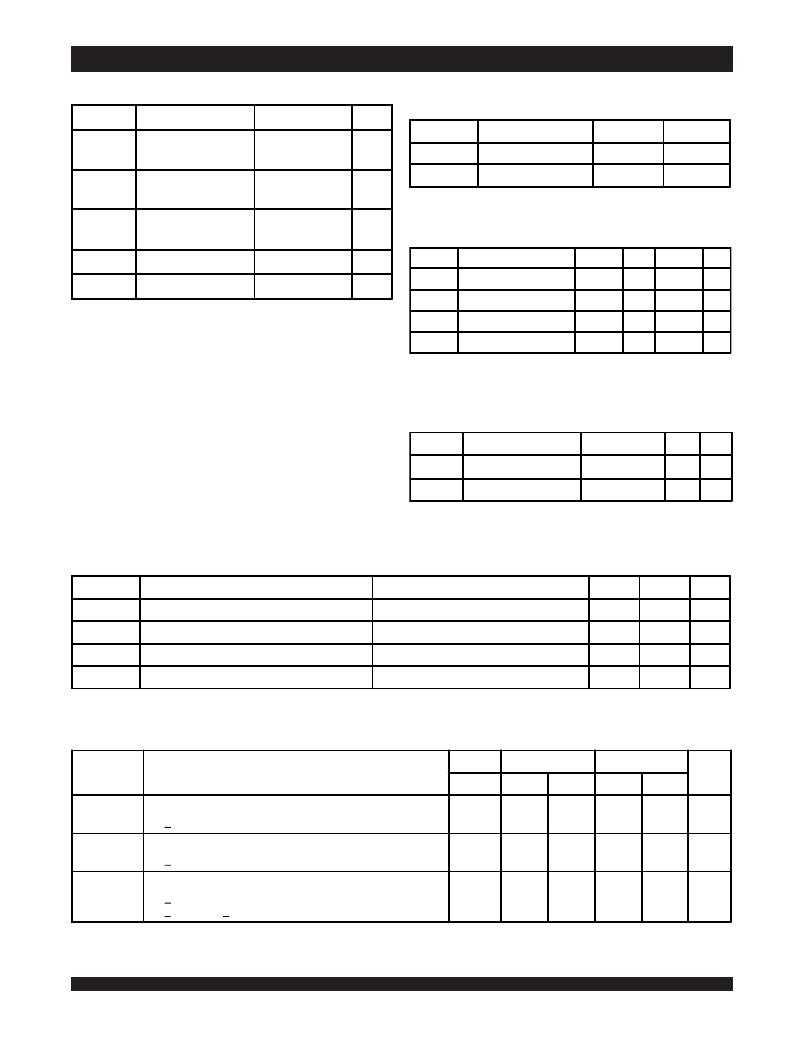
Absolute Maximum Ratings (1)
Symbol Rating Value
Unit
Recommended Operating
Temperature and Supply Voltage
V TERM (2)
Terminal Voltage with
Respect to GND
-0.5 to +7.0
V
Grade
Commercial
Temperature
0°C to +70°C
GND
0V
V CC
5.0V ± 10%
T BIAS
Temperature
-55 to +125
o
C
Industrial
–40°C to +85°C
0V
5.0V ± 10%
Under Bias
3210 tbl 04
T STG
Storage
Temperature
-55 to +125
o
C
Recommended DC Operating
Conditions
P T
I OUT
Power Dissipation
DC Output Current
1.25
50
W
mA
Symbol
V CC
Parameter
Supply Voltage
Min.
4.5
Typ.
5.0
Max.
5.5
Unit
V
3210 tbl 03
NOTES:
1. Stresses greater than those listed under ABSOLUTE MAXIMUM RATINGS may
cause permanent damage to the device. This is a stress rating only and functional
GND
V IH
V IL
Ground
Input High Voltage
Input Low Voltage
0
2.2
-0.5 (1)
0
____
____
0
V DD +0.5
0.8
V
V
V
operation of the device at these or any other conditions above those indicated in the
operational sections of this specification is not implied. Exposure to absolute maximum
rating conditions for extended periods may affect reliability.
NOTE:
1. V IL (min.) = –1.5V for pulse width less than tRC/2, once per cycle.
3210 tbl 05
2. V TERM must not exceed V CC + 0.5V.
Capacitance
(T A = +25° C, f = 1.0MHz, SOJ/TSOP Package)
Symbol
C IN
C I/O
Parameter (1)
Input Capacitance
I/O Capacitance
Conditions
V IN = 3dV
V OUT = 3dV
Max.
6
7
Unit
pF
pF
NOTE:
3210 tbl 06
DC Electrical Characteristics
1. This parameter is guaranteed by device characterization, but not production
tested.
(V CC = 5.0V ± 10%, Commercial and Industrial Temperature Range)
Symbol
|I LI |
|I LO |
V OL
V OH
Parameter
Input Leakage Current
Output Leakage Current
Output Low Voltage
Output High Voltage
Test Conditions
V CC = Max., V IN = GND to V CC
V CC = Max., CS = V IH , V OUT = GND to V CC
I OL = 8mA, V CC = Min.
I OH = -4mA, V CC = Min.
Min.
___
___
___
2.4
Max.
5
5
0.4
___
Unit
μA
μA
V
V
3210 tbl 07
DC Electrical Characteristics (1)
(V CC = 5.0V ± 10%, V LC = 0.2V, V HC = V CC –0.2V)
71016S12
71016S15
71016S20
Symbol
I CC
I SB
I SB1
Parameter
Dynamic Operating Current
CS < V IL , Outputs Open, V CC = Max., f = f MAX (2)
Standby Power Supply Current (TTL Level)
CS > V IH , Outputs Open, V CC = Max., F = f MAX (2)
Standby Power Supply Current (CMOS Level)
CS > V HC , Outputs Open, V CC = Max., f = 0 (2)
Com'l.
210
60
10
Com'l.
180
50
10
Ind.
180
50
10
Com'l.
170
45
10
Ind.
170
45
10
Unit
mA
mA
mA
V IN < V LC or V IN > V HC
NOTES:
1. All values are maximum guaranteed values.
2. f MAX = 1/t RC (all address inputs are cycling at f MAX ); f = 0 means no address input lines are changing .
3
6.42
3210 tbl 08
发布紧急采购,3分钟左右您将得到回复。
相关PDF资料
IDT71024S25TYGI
IC SRAM 1MBIT 25NS 32SOJ
IDT71124S20YGI
IC SRAM 1MBIT 20NS 32SOJ
IDT71256L35Y/2996
IC SRAM 256KBIT 35NS 28SOJ
IDT71256SA25PZGI
IC SRAM 256KBIT 25NS 28TSOP
IDT71321LA20TFG
IC SRAM 16KBIT 20NS 64STQFP
IDT71342LA25PFI
IC SRAM 32KBIT 25NS 64TQFP
IDT7134LA25JI
IC SRAM 32KBIT 25NS 52PLCC
IDT7140LA55C
IC SRAM 8KBIT 55NS 48DIP
相关代理商/技术参数
IDT71016S20YGI8
功能描述:IC SRAM 1MBIT 20NS 44SOJ RoHS:是 类别:集成电路 (IC) >> 存储器 系列:- 标准包装:72 系列:- 格式 - 存储器:RAM 存储器类型:SRAM - 同步 存储容量:4.5M(256K x 18) 速度:133MHz 接口:并联 电源电压:3.135 V ~ 3.465 V 工作温度:0°C ~ 70°C 封装/外壳:100-LQFP 供应商设备封装:100-TQFP(14x20) 包装:托盘
IDT71016S20YI
功能描述:IC SRAM 1MBIT 20NS 44SOJ RoHS:否 类别:集成电路 (IC) >> 存储器 系列:- 产品变化通告:Product Discontinuation 26/Apr/2010 标准包装:136 系列:- 格式 - 存储器:RAM 存储器类型:SRAM - 同步,DDR II 存储容量:18M(1M x 18) 速度:200MHz 接口:并联 电源电压:1.7 V ~ 1.9 V 工作温度:0°C ~ 70°C 封装/外壳:165-TBGA 供应商设备封装:165-CABGA(13x15) 包装:托盘 其它名称:71P71804S200BQ
IDT71016S20YI8
功能描述:IC SRAM 1MBIT 20NS 44SOJ RoHS:否 类别:集成电路 (IC) >> 存储器 系列:- 产品变化通告:Product Discontinuation 26/Apr/2010 标准包装:136 系列:- 格式 - 存储器:RAM 存储器类型:SRAM - 同步,DDR II 存储容量:18M(1M x 18) 速度:200MHz 接口:并联 电源电压:1.7 V ~ 1.9 V 工作温度:0°C ~ 70°C 封装/外壳:165-TBGA 供应商设备封装:165-CABGA(13x15) 包装:托盘 其它名称:71P71804S200BQ
IDT71024MS15Y
功能描述:IC SRAM 1MBIT 15NS 32SOJ RoHS:否 类别:集成电路 (IC) >> 存储器 系列:- 产品变化通告:Product Discontinuation 26/Apr/2010 标准包装:136 系列:- 格式 - 存储器:RAM 存储器类型:SRAM - 同步,DDR II 存储容量:18M(1M x 18) 速度:200MHz 接口:并联 电源电压:1.7 V ~ 1.9 V 工作温度:0°C ~ 70°C 封装/外壳:165-TBGA 供应商设备封装:165-CABGA(13x15) 包装:托盘 其它名称:71P71804S200BQ
IDT71024MS15Y8
功能描述:IC SRAM 1MBIT 15NS 32SOJ RoHS:否 类别:集成电路 (IC) >> 存储器 系列:- 产品变化通告:Product Discontinuation 26/Apr/2010 标准包装:136 系列:- 格式 - 存储器:RAM 存储器类型:SRAM - 同步,DDR II 存储容量:18M(1M x 18) 速度:200MHz 接口:并联 电源电压:1.7 V ~ 1.9 V 工作温度:0°C ~ 70°C 封装/外壳:165-TBGA 供应商设备封装:165-CABGA(13x15) 包装:托盘 其它名称:71P71804S200BQ
IDT71024S12TY
功能描述:IC SRAM 1MBIT 12NS 32SOJ RoHS:否 类别:集成电路 (IC) >> 存储器 系列:- 产品变化通告:Product Discontinuation 26/Apr/2010 标准包装:136 系列:- 格式 - 存储器:RAM 存储器类型:SRAM - 同步,DDR II 存储容量:18M(1M x 18) 速度:200MHz 接口:并联 电源电压:1.7 V ~ 1.9 V 工作温度:0°C ~ 70°C 封装/外壳:165-TBGA 供应商设备封装:165-CABGA(13x15) 包装:托盘 其它名称:71P71804S200BQ
IDT71024S12TY8
功能描述:IC SRAM 1MBIT 12NS 32SOJ RoHS:否 类别:集成电路 (IC) >> 存储器 系列:- 产品变化通告:Product Discontinuation 26/Apr/2010 标准包装:136 系列:- 格式 - 存储器:RAM 存储器类型:SRAM - 同步,DDR II 存储容量:18M(1M x 18) 速度:200MHz 接口:并联 电源电压:1.7 V ~ 1.9 V 工作温度:0°C ~ 70°C 封装/外壳:165-TBGA 供应商设备封装:165-CABGA(13x15) 包装:托盘 其它名称:71P71804S200BQ
IDT71024S12TYG
功能描述:IC SRAM 1MBIT 12NS 32SOJ RoHS:是 类别:集成电路 (IC) >> 存储器 系列:- 标准包装:1 系列:- 格式 - 存储器:闪存 存储器类型:闪存 - NAND 存储容量:4G(256M x 16) 速度:- 接口:并联 电源电压:2.7 V ~ 3.6 V 工作温度:0°C ~ 70°C 封装/外壳:48-TFSOP(0.724",18.40mm 宽) 供应商设备封装:48-TSOP I 包装:Digi-Reel® 其它名称:557-1461-6
